Kelvin

Product Description
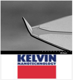
Scanning thermal microscopy probe with integrated Palladium resistance thermometer for thermal mapping in contact mode. The tip can be heated to map thermal conductivity on passive samples, or biased to measure local hotspots.
The probes offer the following features:
Visible tip cantilever
Resistance thermometer located at the tip apex.
Resistance 250 to 400 Ω (typ 320 Ω)
Sensitivity 1 Ω / ºC (approx)
Silicon nitride cantilever (400nm thick)
Tall tip height (~10um) for high aspect ratio features
Fine tip (<100nm radius) for high resolution thermal measurements.
Measure tip resistance with simple Wheatstone bridge or apply apply an A.C. signal and use lock in detector.
Electrical connection is made to two Au pads on the probes base by either wire bonding, conducting epoxy/paste or mechanical clips.
Other applications include applying single point voltages, providing local current stimulus, or detecting thermal properties resulting in cantilever deflections (not generally suitable for scanning un-insulated electrically active samples without electronics to float the probe potential).
Coating Description
Resistive Tip Coating of 5nm NiCr and 40nm Palladium. Tip side track and pad coating of 5nm NiCr + 140nm and series resistor coatings of NiCr (33nm).
Full Technical Data
